Call us now :07971891537( PIN:859)

 Send Inquiry
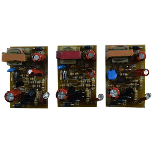
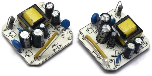
Mobile Charger PCB
Price 11 INR/ Piece
MOQ : 1000 Pieces
Mobile Charger PCB Specification
- Part Type
- PCB
- Model
- Mobile Charger PCB
- Body Material
- PVC
Mobile Charger PCB Trade Information
- Minimum Order Quantity
- 1000 Pieces
- Payment Terms
- Cash in Advance (CID)
- Supply Ability
- 10000 Pieces Per Month
- Delivery Time
- 5-7 Days
- Main Domestic Market
- All India
About Mobile Charger PCB
Seize the opportunity with this limited-time offer on our sizzling Mobile Charger PCB, crafted for those who demand immaculate quality. With input voltages ranging between 1000-14000 mV and monumental output spanning 10000-135000 mV, this PCB sets an uncommon standard for mobile charging solutions. Built using superior SMD components and robust PVC, it combines single-layer efficiency with user-friendly through-hole mounting. Whether you are a manufacturer, supplier, or trader across India, pick yours today and experience a leap in reliability and performance!
Precision Mobile Charging: Usage and Application Benefits
Designed specifically for mobile charging circuits, this Mobile Charger PCB simplifies electronic assembly with its through-hole mounting. The PCB uses top-tier SMD components and features a single-layer design, making installation straightforward. Its PVC body ensures durability, while the monumental voltage range supports diverse charging needs. Ideal for manufacturers, traders, or DIY repairers, the PCB's advantage lies in its simplicity, reliability, and efficiency, boosting your productivity during assembly or repair tasks.
Swift Delivery and Reliable Supply for Every Valuation
Enjoy prompt delivery of your Mobile Charger PCB with dependable timelines and transparent valuation. Products are dispatched from major Indian FOB ports, ensuring seamless shipment wherever you are located. With strong supply ability, large or small orders are handled efficiently by the manufacturer, supplier, and trader network. Rely on our service to have your mobile charger PCBs delivered punctually, no matter the size of your requirement, supporting your business with consistent availability and quality.
FAQ's of Mobile Charger PCB:
Q: How do I install the Mobile Charger PCB in my circuit?
A: Installation is straightforward using the through-hole mount type. Simply align the PCB on your board, insert the pins, and solder them securely. This ensures solid connectivity and stable performance with minimum hassle.Q: What distinguishes this Mobile Charger PCB from conventional circuits?
A: This PCB offers an uncommon voltage compatibility, supporting input voltages from 1000-14000 mV and output voltages up to 135000 mV. It uses immaculate SMD components on a single-layer PVC board, providing reliability and efficiency for diverse charging needs.Q: When can I expect delivery after placing an order?
A: Typically, delivery is prompt and handled from major Indian FOB ports. The exact delivery time will depend on your location and the size of your order, but prompt shipment and handling are prioritized.Q: Where is the Mobile Charger PCB manufactured and supplied?
A: These PCBs are manufactured, supplied, and traded across India, with distribution supported from key Indian ports to reach customers efficiently, no matter their location in the country.Q: What applications is this PCB best suited for?
A: The Mobile Charger PCB is designed for use in mobile charging circuits. It is suitable for both manufacturers assembling new devices and technicians involved in repair, providing a reliable and high-output solution.Q: What is the benefit of using a single-layer, SMD component PCB?
A: Single-layer PCBs with SMD components offer higher reliability, easier mounting, and faster assembly. This design reduces potential circuit errors and increases durability while keeping the manufacturing process cost-effective.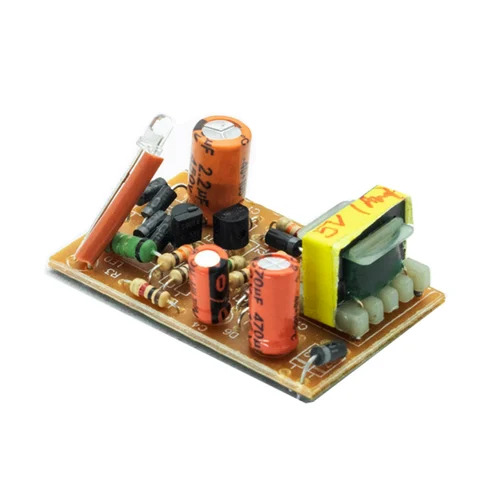
More Products in Mobile Charger Parts Category
Mobile Charger Cabinet
Price 3 INR / Piece
Minimum Order Quantity : 1000 Pieces
Body Material : Metal Sheet
Color : Black
Accessories Type : Lock & Key
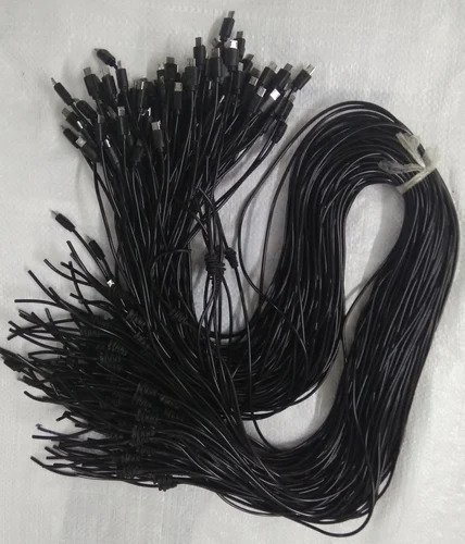
Mobile Charger Wire
Price 4 INR / Piece
Minimum Order Quantity : 1000 Pieces
Body Material : PVC
Color : Black
Accessories Type : Mobile Charger Wire
Part Type : Charging Cable
2.5 Amp Smd Double Usb Charger Pcb
Price 40 INR / Piece
Minimum Order Quantity : 1000 Pieces
Body Material : Copper
Color : Green PCB
Part Type : Charger PCB
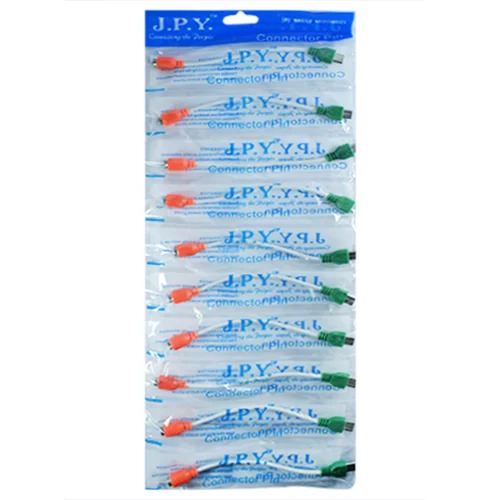
Mobile Charger Connector Pin
Price 3.5 INR / Piece
Minimum Order Quantity : 1000 Pieces
Body Material : PVC
Color : Tricolor
Accessories Type : Mobile Charger Connector Pin
Part Type : Connector Pin
Our Products
- MOBILE DATA CABLE
- Power Bank
- DC Power Cord
- Rechargeable Torch
- Motion Sensor Light
- Diwali Diya
- Dc Cooling Fan
- Face Mask
- Cable Tester
- Pulse Oximeter
- Universal Charger
- Door Lock
- Plastic Bottle
- Children Camera
- Digital Camera
- Support Bracket
- Car Stand
- Wifi Camera
- Night Lamp
- Usb Data Cable
- Mobile Ring Holder
- Fidget Spinner
- Data Cable
- Dc Pin
- BNC Connector
- Computer Cable
- Led Night Lamp
- Led Diya
- Mobile Cover
- Memory Card Readers
- USB LED Light
- Jewellery Display Racks And Stands
- Electric Cables
- Power Cord
- Display Stands
- Promotional Toys
- OTG Cable
- USB Fan
- Kids Toys
- Screen Cleaner
- Stylus Pen
- HDMI Cables
- Selfie Stick
- Smart Watch
- Telephone Cables
- Bluetooth Speaker
- Mobile Battery
- LED Ring Light
- Extension Cable
- Portable Speaker
- Mobile Earphones
- AV Cables
- Aux Cable
- Camera Tripod
- Mobile Charger Parts
- Charging Pin
- OTG Cables
- Pen Drive Chip
- Mobile Accessories
- Mobile Stand
- Mobile Chargers
- Micro Usb Data Cable
- Usb Charger
- Air Cooler
- Alarm Lock

F-119, Punjabi Basti, Baljeet Nagar, Opposite Sitaram Mandir,New Delhi - 110008, India

Mr. Ajay
(Director)
Mobile :917971891537 PIN:( 859 )
 Send Inquiry
 Send SMS
Developed and Managed by Infocom Network Private Limited.


